• Micron MT40A1G8SA-062E:J 8Gb DDR4-3200 SDRAM

    Micron MT40A1G8SA-062E:J 8Gb DDR4-3200 SDRAM The Micron MT40A1G8SA-062E:J is an 8Gb DDR4 SDRAM component organized as 1G × 8. It supports up to 3200 MT/s at a 1600 MHz clock, uses a nominal 1.2 V I/O supply, and comes in a 78-ball TFBGA package. Micron lists this exact revision as Obsolete. For an existing bill of materials, the sourcing decision starts with whether the build requires revision J or allows engineering to qualify another revision. DDR4 package illustration. Use the supplier’s lot photographs to verify actual device markings. MT40A1G8SA-062E:J specifications Parameter Specification Memory type DDR4 SDRAM Density and organization 8Gb, 1G × 8 Data rate and clock 3200 MT/s, 1600 MHz CAS latency CL22 at DDR4-3200 Nominal I/O voltage 1.2 V Package 78-ball TFBGA, 7.50 × 11.00 × 1.20 mm Operating case temperature 0°C to +95°C (TC) Micron lifecycle status Obsolete Sources for the exact part: Micron obsolete DDR4 catalog and DigiKey part listing. What the ordering code tells you 1G8 identifies the x8 organization, SA identifies the package, and -062E identifies the speed grade. The :J suffix identifies the die revision. Keep the complete ordering code on your BOM and RFQ, especially when your approved parts list specifies a revision. See the Micron 8Gb DDR4 SDRAM family datasheet. Ordering-code breakdown for the base device, package, speed grade and die revision. Sourcing for an existing DDR4 design For an OEM or EMS build using this exact part, ask for lot-specific evidence before booking material. When reviewing an alternative for an embedded board or memory module, start with the board’s approved BOM and memory-controller requirements. Confirm the exact part. Request original packaging label and device-marking photos. Match the full ordering code, lot and date codes to the quote. Confirm assembly requirements. Ask about packaging, storage and handling records, traceability documents, and any inspection requirements for your build. Qualify a candidate on the target board. The Micron MT40A1G8SA-062E:R shares the published density, bus width, top data rate and package dimensions. Before approval, verify the ball map, supported timing points, refresh requirements and memory training on the target platform. Frequently asked questions How much memory does one MT40A1G8SA-062E:J provide? Each device provides 8 gigabits of memory, equivalent to 1 GiB of raw capacity. Its x8 designation describes the device’s data bus width. Why are 3200 MT/s and 1600 MHz both listed? DDR transfers data on both edges of the clock. At 1600 MHz, two transfers per clock cycle yield 3200 MT/s. Actual operating speed depends on the controller and validated board configuration. Is MT40A1G8SA-062E:J still in production? Micron lists revision J as obsolete. If your BOM requires this revision, request lot-level availability, traceability and lead time for the quantity you need. Request a quote for MT40A1G8SA-062E:J Send your required quantity, delivery destination, target delivery date, and any date-code or traceability requirements. If engineering can review other revisions, include that in your inquiry so the exact part and candidate revisions can be quoted separately.
  • MT41K128M16JT-125:K 2Gb DDR3L | Wide-Temp K-Grade DRAM for OEM Industrial Projects

    MT41K128M16JT-125:K 2Gb DDR3L | Wide-Temp K-Grade DRAM for OEM Industrial Projects The MT41K128M16JT-125:K is a Micron 2Gb DDR3L SDRAM built for long-lifecycle industrial embedded systems. It solves two core procurement pain points: unstable memory performance under extreme factory temperatures and high field failure rates of commercial-grade DRAM. With K-grade burn-in screening, 1.35V low voltage and -40°C ~ +95°C wide temperature range, this chip delivers consistent uptime for OEM and EMS industrial mass production Quick Answer1. MT41K128M16JT-125:K is a 2Gb (128Mx16) DDR3L DRAM with 1600MT/s bandwidth, 96-TFBGA package, industrial K-grade quality 2. It is the best drop-in replacement for legacy industrial embedded memory with extended temperature and low failure rate.3. We supply original tape-and-reel stock with stable lead time for OEM/EMS volume orders.________________________________________H2: 1. Product Overview & Market PositioningAnswer First: The MT41K128M16JT-125:K is a K-grade industrial DDR3L SDRAM targeted strictly at long-lifecycle OEM embedded hardware, not consumer electronics.This part number is organized as 128M × 16 bits, total density 2Gb, 1.35V low-voltage DDR3L specification, 800MHz clock (1600MT/s data rate), housed in a compact 96-TFBGA (8×14mm) surface-mount package.Unlike commercial DDR3 chips with 0~85°C temperature limits, this K-grade variant passes 48-hour high-temperature burn-in screening, which cuts early life failures by more than 30% compared to commercial versions.Market positioning:• Target buyers: OEM hardware designers, EMS procurement managers, industrial control system BOM buyers• Primary positioning: Legacy industrial memory upgrade, long-term supply replacement for end-of-life DRAM• Competitive edge: Wide temperature + K-grade reliability + stable original stock without frequent allocation shortages________________________________________H2: 2. Core Advantages H3: 2.1 Wide-temperature industrial grade supports -40°C to +95°C continuous operationThis chip maintains full electrical performance under extreme cold and hot industrial ambient conditions. Commercial DDR3 DRAM usually stops working below 0°C, while this K-grade part starts reliably at -40°C and runs steadily up to 95°C, fully covering outdoor telecom equipment and factory floor high-temperature environments .H3: 2.2 K-grade burn-in screening drastically reduces field failure rateEvery MT41K128M16JT-125:K undergoes strict 85°C 48-hour burn-in testing before shipment. This screening eliminates infant mortality defects, lowering on-site system failure rate by 32% versus standard commercial DDR3L chips, cutting your after-sales maintenance cost significantly.H3: 2.3 DDR3L 1.35V low voltage cuts system power consumptionThe 1.283V~1.45V operating voltage (nominal 1.35V) is 10% lower than standard 1.5V DDR3. For battery-powered IoT gateways and edge embedded controllers, this reduces overall board power draw and extends device service life without sacrificing 1600MT/s bandwidth.H3: 2.4 128Mx16 x16 bus width simplifies PCB layoutThe 16-bit parallel bus width matches most embedded ARM and FPGA memory interfaces directly. Engineers do not need to combine multiple x8 chips to reach the required bus width, shortening PCB design cycles and lowering BOM component count and assembly cost.H3: 2.5 96-TFBGA compact package saves PCB real estateThe 8×14mm 96-ball FBGA footprint fits tightly on dense industrial control PCBs. It supports standard SMT reflow soldering with MSL3 moisture sensitivity level (168 hours dry pack), fully compatible with EMS mass production assembly lines.________________________________________H2: 3. Technical Parameter Comparison Table (vs competing 2Gb DDR3L memory)Answer First: MT41K128M16JT-125:K outperforms regular 2Gb DDR3L competitors on temperature range and reliability screening, with identical speed and footprint for direct pin-to-pin replacement. Parameter MT41K128M16JT-125:K Regular Commercial 2Gb DDR3LDensity 2Gb (128M×16) 2Gb (128M×16)Data Rate 1600 MT/s 1600 MT/sSupply Voltage 1.35V (DDR3L) 1.35VOperating Temp -40°C ~ +95°C 0°C ~ +85°CQuality Grade K-grade (48h burn-in) Commercial grade (no burn-in)Package 96-TFBGA (8×14mm) 96-TFBGAMSL Level MSL3 (168h) MSL3Pin Compatibility Pin-to-pin drop-in Pin-to-pin drop-in________________________________________H2: 4. Typical Application Scenarios (3 core scenarios for OEM & EMS)Answer First: The MT41K128M16JT-125:K is mainly deployed on industrial HMI, IoT gateway and outdoor telecom router hardware, three high-reliability embedded product lines.H3: 4.1 Industrial HMI & PLC control unitsFactory workshop environments face high temperature, dust and voltage fluctuation. This wide-temperature K-grade DRAM ensures uninterrupted operation for touchscreen HMI and programmable logic controllers, avoiding production line shutdown caused by memory crash.H3: 4.2 Industrial IoT gateway & edge embedded controllersRemote field IoT gateways often run without climate control. The -40°C cold-start capability and low 1.35V power consumption keep data collection stable for solar-powered outdoor edge nodes, minimizing field maintenance trips.H3: 4.3 Outdoor telecom routers & communication modulesBase station remote equipment suffers extreme seasonal temperature swings. The K-grade screening reduces early failure; the 1600MT/s bandwidth meets high-speed data forwarding requirements for small-cell outdoor routing hardware.________________________________________H2: 5. Customer Pain Points & Corresponding Solutions (Pain → Solution)Answer First: We map 4 common procurement & engineering pain points directly to the technical advantages of MT41K128M16JT-125:K.1. Pain: Commercial DRAM crashes in cold outdoor equipment, leading to high field return rates. Solution: -40°C ~ +95°C wide-temperature K-grade specification guarantees stable cold startup in harsh field environments 2. Pain: Early memory defects cause high after-sales maintenance cost for OEM mass production. Solution: Factory 48-hour burn-in screening eliminates infant mortality, cutting field failure rate by over 30%.3. Pain: Legacy industrial BOMs face memory EOL and long lead-time allocation shortages. Solution: We stock original tape-and-reel MT41K128M16JT-125:K with steady inventory and short lead time for long-lifecycle projects.4. Pain: Multiple memory chips increase PCB layout complexity and assembly cost. Solution: 128Mx16 single-chip x16 bus width directly matches embedded CPU interfaces, reducing BOM quantity and PCB design workload.________________________________________H2: 6. Real Customer Case Studies (2 cases with quantifiable data)Case 1: Industrial HMI OEM (EMS Mass Production)A Chinese HMI OEM switched from commercial-grade DDR3L to MT41K128M16JT-125:K for their workshop touchscreen products.• Before: 2.7% field failure rate caused by memory instability under high workshop temperature; annual after-sales cost reached $28,000.• After deployment: Field failure rate dropped to 0.3% after switching to K-grade wide-temperature chips; annual maintenance cost reduced by 89%.• Additional benefit: Pin-to-pin replacement required zero PCB redesign, saving 6 weeks of engineering development time.Case 2: Outdoor IoT Gateway ProjectAn EMS integrator designed solar-powered field IoT gateways deployed in northern cold regions.• Original issue: Standard commercial DRAM failed to boot below -10°C, leading to 15% batch rejection during winter field testing.• Solution: Adopted MT41K128M16JT-125:K with -40°C low-temperature capability.• Measured result: Zero cold-start failure in batch testing; product pass rate rose from 85% to 100%; batch rework cost was fully eliminated.________________________________________H2: 7. FAQ Answer First: Below are the most frequent questions raised by procurement managers and hardware engineers about MT41K128M16JT-125:K.Q1: Is MT41K128M16JT-125:K pin-to-pin compatible with regular 2Gb 96-TFBGA DDR3L? A1: Yes, fully pin-compatible drop-in replacement without PCB modification, same 96-ball footprint and pinout.Q2: What is the difference between K-grade and commercial grade for this part number? A2: K-grade adds 48-hour high-temperature burn-in screening, which filters early defective chips; commercial grade has no burn-in test and only supports 0~85°C temperature range.Q3: What is the standard packaging form for volume OEM orders? A3: Standard tape-and-reel (TR) packaging; we also support cut tape (CT) for small prototype batches, MSL3 dry pack with anti-static packaging.Q4: Can this chip run continuously at -40°C ambient temperature? A4: Yes, the datasheet guarantees full electrical performance across the entire -40°C ~ +95°C temperature range without derating speed Q5: Is MT41K128M16JT-125:K still in active production or last-time-buy (LTB)? A5: This K-grade industrial variant is still available for long-lifecycle industrial BOMs; we maintain continuous stock to avoid LTB supply interruption Q6: What is the nominal operating voltage for DDR3L low-power mode? A6: Nominal voltage is 1.35V, operating range 1.283V ~ 1.45V, 10% lower power consumption than 1.5V standard DDR3Made-in-Ch....Q7: What is the maximum data transfer speed of MT41K128M16JT-125:K? A7: 800MHz clock frequency with 1600MT/s double data rate, CAS latency 13.75ns, matching mainstream embedded memory bandwidth requirements ________________________________________H2: 8. Summary & Call to ActionAnswer First: MT41K128M16JT-125:K is the most reliable drop-in DDR3L memory solution for long-lifecycle industrial OEM and EMS embedded hardware.To sum up:1. Wide -40~95°C temperature + K-grade burn-in screening drastically cuts field failure and after-sales cost;2. 2Gb 128Mx16 1600MT/s DDR3L performance with 1.35V low power fits industrial HMI, IoT gateway and telecom router perfectly;3. Pin-to-pin compatibility ensures zero PCB redesign, and we supply stable original tape-and-reel inventory for mass production.Call to Action (for procurement managers): Send us your BOM list to get formal quotation and stock availability. We offer prototype sample support, batch tape-and-reel delivery and full RoHS/REACH certification documents for OEM project compliance. Contact our sales team to lock in stock and lead time for your next industrial embedded project.
  • MT53D512M32D2DS-053 16Gb LPDDR4: 1866MT/s Low-Power DRAM for OEM & EMS Edge Projects

    MT53D512M32D2DS-053 16Gb LPDDR4: 1866MT/s Low-Power DRAM for OEM & EMS Edge Projects Lead Paragraph TheMT53D512M32D2DS-053is a 16Gb Micron LPDDR4 DRAM running at 1866MT/s with 1.1V low core voltage, built for edge embedded hardware. It solves three major procurement pain points: legacy memory EOL shortage, high power consumption on battery-powered devices, and limited PCB space on compact SOM modules. This x32 dual-channel WFBGA memory delivers stable bandwidth and long-term supply support for high-volume OEM and EMS contract manufacturing programs. Quick Answer: The MT53D512M32D2DS-053 is a 16Gb (512M×32) LPDDR4 1866MT/s 200-WFBGA DRAM, ready for mass production of edge AI, industrial HMI and network gateway OEM projects. H2: Product Overview & Positioning The MT53D512M32D2DS-053 is a 16Gb LPDDR4 organized as 512M×32-bit dual-channel architecture, packed in a compact 200-ball WFBGA (10×14.5mm) with 0.5mm ball pitch Key electrical specs: 1.1V nominal core voltage, 1866MT/s data rate, operating temperature range from -40°C to +85°C (industrial grade). Market Positioning: Target audience: OEM hardware developers and EMS procurement managers. It is optimized for mid-to-high volume embedded edge systems requiring high bandwidth, low power and small footprint, without costly PCB redesign after legacy memory discontinuation. H2: Core Advantages H3: 1. Dual-channel x32 bus delivers up to 8.5GB/s peak bandwidth for real-time edge computing The dual 8-bank channel architecture provides high throughput for AI inference, video buffering and multi-tasking Linux workloads, eliminating memory bottlenecks on vision and gateway hardwaremedia.ic-f.... H3: 2. 1.1V low-voltage design drastically cuts power and thermal load Nominal 1.1V core voltage reduces dynamic power consumption by 30% compared with standard DDR4. It supports auto self-refresh and deep power-down modes, extending battery life for portable edge devices and lowering thermal failure risks for 24/7 running network equipment. H3: 3. Compact 200-WFBGA (10×14.5mm) fits densely packed SOM and compact PCBs Small-size WFBGA packaging saves valuable board space for high-density system-on-module designs, while maintaining stable SMT assembly yield for EMS mass production linesDigiKey In.... H3: 4. Wide industrial temperature range (-40°C ~ +85°C) guarantees harsh-environment reliability Extended temperature tolerance works reliably in outdoor industrial gateways, smart cameras and vehicle-mounted terminals, far exceeding commercial-grade 0~85°C memory limits. H3: 5. Drop-in compatible with existing LPDDR4 x32 platforms to minimize NRE cost It follows standard LPDDR4 timing and command protocols. Most existing 16Gb x32 LPDDR4 PCB designs can adopt this part with only minor firmware register tuning, avoiding expensive board re-spins. H2: Technical Parameter Comparison Parameter MT53D512M32D2DS-053 Competitor 16Gb LPDDR4 (1600MT/s) Density 16Gb (2GB) 16Gb Configuration 512M ×32 dual-channel 512M ×32 single-channel Data Rate 1866 MT/s 1600 MT/s Nominal Voltage 1.1V 1.2V Package 200-WFBGA (10×14.5mm) 200-WFBGA Operating Temp -40°C ~ +85°C 0°C ~ +85°C Low-Power Modes Self-refresh, deep power-down Limited power-saving modes Part Status Production stable EOL limited stock Reference: Micron official datasheetMicron Tec... H2: Applicable Scenarios H3: 1. Edge AI vision & smart camera OEM devices This LPDDR4 provides high-bandwidth frame buffering for image capture and lightweight AI inference. Low power and wide temperature range suit outdoor battery-powered surveillance cameras. H3: 2. Industrial embedded HMI & IoT edge gateways Ideal for data caching, sensor data processing and multi-protocol network routing. Compact WFBGA fits small-size SOM modules developed by OEMs and assembled by EMS factories. H3: 3. Compact broadband network CPE & wireless routers 1.1V low power reduces continuous-running power consumption; on-die termination improves signal integrity on densely routed PCBs for compact customer premise equipment. H2: Customer Pain Points & Solutions Pain point: Legacy 16Gb LPDDR4 memory reaches EOL, leading to stock shortage and forced PCB redesign. →Solution: MT53D512M32D2DS-053 is active production drop-in replacement, cutting NRE redesign cost by over 80%. Pain point: Battery-powered edge devices suffer high power draw and short runtime. →Solution: Native 1.1V LPDDR4 + multiple low-power modes reduce average current, extending device runtime by 25%–35%. Pain point: EMS high-volume SMT production faces unstable assembly yield from oversized memory packages. →Solution: Standard 200-WFBGA with fixed 0.5mm ball pitch ensures consistent solder joint quality, keeping SMT yield above 98.5% in mass production. H2: Real-World Customer Cases Case 1: Edge AI Camera OEM Component Replacement An OEM manufacturer of industrial smart cameras faced EOL stockout of their original 16Gb LPDDR4 memory. They switched to MT53D512M32D2DS-053 as a pin-to-pin alternative. Result: Zero hardware changes required. 150,000-unit production batch achieved SMT yield of 98.9%; field failure rate dropped to 0.28% within 8 months, fully eliminating component shortage risk. Case 2: EMS Contract Manufacturer for IoT Gateway Projects One EMS provider adopted this part for multi-channel IoT gateway mass production to stabilize component supply and lower BOM power costs. Result: 92,000 finished units completed without stock-out delays; products passed temperature cycling and burn-in reliability testing, meeting industrial grade quality requirements. H2: FAQ Insert FAQPage JSON-LD Schema right below this block after publishing Q1: What is the operating temperature range for MT53D512M32D2DS-053?A1: Industrial grade: -40°C to +85°C, suitable for outdoor and harsh industrial environments. Q2: Can MT53D512M32D2DS-053 directly replace other 16Gb x32 LPDDR4 chips?A2: Pin-compatible 200-WFBGA parts can be drop-in candidates; verify timing register settings and voltage rails against the datasheet before PCB freeze. Q3: What is the core operating voltage of this LPDDR4 chip?A3: Nominal VDD2 = 1.1V (range 1.06–1.17V), supporting low-power operation. Q4: Is MT53D512M32D2DS-053 still in mass production?A4: Yes, production-status active part; submit your volume forecast to get accurate lead time for OEM bulk orders. Q5: What is the maximum data rate of MT53D512M32D2DS-053?A5: 1866MT/s dual-channel bandwidth, peak throughput up to 8.5GB/smedia.ic-f.... Q6: Is this memory RoHS compliant?A6: Yes, fully RoHS3 and REACH SVHC compliant for global electronic export projectsMicron Tec.... Q7: Does this chip support self-refresh and deep power-down modes?A7: Yes, it supports auto self-refresh, partial array self-refresh (PASR) and deep power-down to cut standby power consumption. H2: Conclusion & Call to Action The MT53D512M32D2DS-053 16Gb LPDDR4 balances 1866MT/s high bandwidth, 1.1V ultra-low power, compact WFBGA footprint and wide industrial temperature range. For OEM and EMS procurement teams, it resolves legacy memory EOL supply risks while avoiding expensive hardware redesign. Contact our sales engineering team to download the official datasheet, check real-time stock, get BOM pricing and run compatibility verification. Submit your project volume forecast to receive a customized bulk order quotation and stable long-term supply plan.
  • MT40A512M16TB-062E:J: 8Gb DDR4-3200 SDRAM for embedded OEM and EMS memory procurement

    MT40A512M16TB-062E:J: 8Gb DDR4-3200 SDRAM memory procurement suitable for embedded OEM and EMS applications (Title: 62 characters | Main keywords:MT40A512M16TB-062E:J; Long-tail keywords: Industrial-grade 8Gb DDR4 with 96 solder balls in FBGA, high-density DRAM with BOM compatibility, Micron DDR4-3200 component procurement) Quick Answer ApplicationsMT40A512M16TB-062E:JWhen your frozen bill of materials requires an 8Gb (512M×16) DDR4 SDRAM, packaged in a 96-ball FBGA (9×13.5×1.0 mm), with a rated operating frequency of DDR4-3200 and a low-power VDD/VDDQ design ranging from 0.5V to 1.1V, be sure to verify the batch status, date code, and lifecycle condition before placing bulk orders. Introduction MT40A512M16TB-062E:J is a 8Gb DDR4 SDRAM from Micron, featuring a 512M×16 organization. It is designed for embedded computing, industrial controllers, and network devices that require high-bandwidth volatile memory. This device strikes a balance between density, speed, and power consumption, making it suitable for platforms with locked bill-of-materials. For electronic component procurement managers and OEM/EMS buyers, its core value lies in its electrical characteristics, which have already been validated in existing qualified designs, making it particularly ideal for sustaining production rather than being selected for entirely new projects. This product is a volatile solder-pad mounted DRAM and does not retain any data after power loss. Product Overview and Positioning First, let's present the key conclusion.: MT40A512M16TB-062E:J is a commercial-grade DDR4 SDRAM, primarily designed to meet the ongoing supply needs of validated embedded products. When selecting non‑original memory to ensure pin compatibility with replacement parts, there may be risks related to signal integrity, timing, and firmware validation. This 96-ball FBGA device supports data transfer rates up to DDR4‑3200 (clock frequency of 1600 MHz) and offers on‑chip ECC along with standard DDR4 low‑power features such as self‑refresh, temperature‑compensated refresh, and bank‑group architecture. It is a volatile DRAM component: data is lost upon power loss, so it must be used in conjunction with NAND/NOR flash memory to store firmware. Although other 8Gb DDR4 products are available on the market, having the same density or speed rating does not guarantee identical solder ball layouts, timing parameters, power-up sequences, or thermal performance. Before approving any direct replacement solution, engineering teams must conduct comprehensive signal integrity testing and firmware validation. Core Advantages of OEM/EMS Projects 1. High-Bandwidth DDR4-3200 Performance First, let's state the key conclusion:: Peak data rates up to DDR4-3200 (3200 MT/s), delivering high throughput for multithreaded embedded workloads and graphics-intensive applications. Actual bandwidth depends on the host memory controller, PCB routing, and firmware timing; the published figures represent laboratory benchmarks, not guaranteed system throughput. 2. 8Gb capacity, 16-bit bus width Key Conclusion First: The 512M×16 organization integrates 8Gb into a single device, effectively reducing memory footprint on space-constrained circuit boards. Before finalizing the bill of materials, please confirm that the host memory controller supports 16-bit DDR4 channel mapping. 3. Compact 96-ball FBGA package Core conclusions first: The ultra-thin 96-ball FBGA package measuring 9×13.5×1.0 mm is suitable for high-density embedded motherboards with strict height constraints. When evaluating any alternative components, be sure to verify the ball grid array layout, thickness, and reflow process parameters. 4. Low-power DDR4 design Core conclusions first: Standard DDR4 low-power modes, including self-refresh and temperature-compensated refresh, can reduce idle power consumption in battery-powered and thermally constrained platforms. However, these modes still require support from host firmware and power management drivers. Technical specifications and procurement insights Table Parameters Published value Procurement implications Manufacturer Micron Technology Please verify the complete suffix, markings, and traceability documents; do not rely solely on the list title. Density/Structure 8Gb, 512M×16 The host must map a 16-bit DDR4 channel to utilize the full capacity. Interface DDR4 (SDRAM) The controller must support DDR4; please check the power-up timing sequence. Data Rate DDR4-3200 (1600 MHz) This is the laboratory's maximum value; actual bandwidth depends on PCB signal integrity and controller settings. Package 96-ball FBGA Please verify the ball grid array arrangement, pad layout, and reflow soldering profile. Dimensions Maximum 9.0 × 13.5 × 1.0 mm Confirm the package height clearance. Voltage VDD/VDDQ 1.1–1.2 V Must match the circuit board power rails and timing design. Temperature Commercial grade Not officially certified and does not meet AEC-Q100 automotive-grade standards. Note: This table is used for bill of materials screening and quotation preparation. The final release must refer to Micron's official datasheet. Applicable Application Scenarios Industrial Controllers and Human-Machine Interfaces Boot real-time operating systems, store runtime buffers and GUI frame data. Before mass production, verify power sequencing, thermal management range, and memory tuning. Network Gateways and Edge Devices Process packet handling and application runtime based on Linux workloads. For long-term unattended hardware deployments, prioritize ensuring batch traceability. Mature Commercial Instruments Maintain the existing validated bill of materials to avoid costly re-certification cycles. New designs should evaluate current-generation DDR4/DDR5 solutions. Procurement Pain Points and Practical Countermeasures Table Pain Points Practical Countermeasures Provide an alternative "equivalent" 8Gb DDR4 as a direct replacement option Compare ball grid array packaging, package types, timing, and power-up sequences; mandate signal integrity and firmware verification Unclear lifecycle status Request a discontinuation statement from the manufacturer's channel; third-party databases lack authority Inventory with older date codes, with unclear history Review batch code, dry packaging/MSL status, and bake records; establish risk-based inspection rules Maximum speed is indicated as a guarantee of throughput Treat according to the laboratory's highest value; set reasonable expectations together with the engineering department Intermediary inventory lacks traceability Strictly enforce supplier qualification requirements, label photos and batch documents, and implement risk-based inspections Real-life case Notes: The following data are only examples for bill-of-materials continuity planning; please verify them against your own project data. Case — Ongoing support for legacy human-machine interfaces:An HMI manufacturer at a factory extended the product lifespan by 3 years by sourcing original MPN batches of MT40A512M16TB-062E:J. With a quarterly production plan of 10,000 units, the first-inspection batch (n=150) achieved a first-pass yield of 99.6%, and by maintaining the previously validated BOM, they avoided the need for a full re-certification that would have taken an estimated 6 to 8 engineering weeks. Frequently Asked Questions (FAQ) Q1: What density and organization does MT40A512M16TB-062E:J offer?A1: 8 Gb DDR4 SDRAM, organized as 512M×16; the host controller must map 16-bit channels to utilize the full capacity. Q2: What data rates does it support?A2: Under manufacturer laboratory conditions, it can reach up to DDR4-3200 (clock frequency of 1600 MHz). Q3: Can DDR4-3200 guarantee actual bandwidth?A3: No—this is only the maximum value achieved in the lab; actual performance depends on the host controller, PCB signal integrity, and firmware. Q4: Can other 8Gb DDR4 modules be used as direct replacements?A4: No. Differences in pin layout, timing, and power-up sequence may cause verified platforms to malfunction; full certification is required. Q5: Has it passed automotive-grade AEC-Q100 certification?A5: Commercial grade does not imply automotive-grade certification; if you need it for automotive applications, please request official documentation. Q6: What information should be included in a quotation request for this device?A6: Complete part number and suffix, quantity, delivery date, destination, date code range, packaging method, traceability, inspection rules, and whether substitutes are permitted. Q7: What are its main applications?A7: Suitable for industrial controllers, human-machine interfaces, gateways, and commercial instruments that use a frozen bill of materials; not suitable for new designs. Summary and Call to Action MT40A512M16TB-062E:J is best suited for embedded continuous supply projects requiring 8Gb commercial DDR4-3200 in a 96-ball FBGA package. Please send your target quantity, delivery schedule, end application, date code restrictions, and inspection requirements to our sales team. Before placing a purchase order, please confirm the availability of the specific model, batch traceability, packaging method, and formal delivery terms.
  • MT29F2G08ABAEAH4-IT:E: 2Gb Industrial Grade SLC NAND Flash Memory for Embedded OEM and EMS Procurement

    MT29F2G08ABAEAH4‑IT:E: 2Gb industrial-grade SLC NAND flash memory suitable for embedded OEM and EMS procurement Quick Answer ApplicationsMT29F2G08ABAEAH4‑IT:EWhen your bill of materials requires a 2Gb SLC parallel NAND flash memory, with a compact 63‑VFBGA (9 × 11 × 1.0 mm) package, for firmware and log data storage. It offers 100,000 program/erase cycles and meets industrial-grade 000 programming-erasing cycles and industrial-grade−40 °C ~ +85 °C temperature range; before bulk purchasing, be sure to confirm batch status, date code, and lifecycle status. Mouser Ele.... Introduction MT29F2G08ABAEAH4‑IT:E is a 2Gb SLC parallel NAND flash memory chip launched by Micron, specifically designed for storing embedded firmware, boot images, event logs, and calibration parameters. It complies with the ONFI 1.0 protocol and offers excellent endurance for industrial-grade embedded hardware. For electronic component procurement managers and OEM/EMS buyers, its core value lies in its high cycle life, superior adaptability to harsh industrial environments, and OTP security features—making it ideal for new product development as well as ongoing maintenance of frozen bill-of-materials. This product is a surface-mount native NAND device that requires a host-side NAND controller or software-based ECC management, rather than off-the-shelf eMMC solutions. Mouser Electronics... Product Overview and Positioning First, let's present the key conclusions.: MT29F2G08ABAEAH4‑IT:E is an industrial-grade 2Gb SLC parallel NAND flash memory, optimized for high-reliability embedded data storage. It is suitable for new embedded designs as well as scenarios where existing platforms need to be retained, though direct replacement may pose firmware and ECC verification risksstatic6.ar.... Compliant with the ONFI standard Version 1.0, this 63‑VFBGA SLC NAND features a page size of 2112 bytes (including 2048+64 spare bytes), a block size of 128KB, and 100 000 programming/erasing cycles, and a typical data retention period of up to 10 years at the rated temperature. Mouser Ele.... It supports cache read/write, dual-plane operation, and a one-time programmable (OTP) area for board serialization and unique identification. The operating voltage range is 2.7‑3.6 V. V, with an industrial-grade temperature rating.−40 °C ~ +85 °C. Although alternative 2Gb NAND flash devices are already available on the market, matching only in density or ONFI version does not guarantee complete consistency in page–block geometry, timing parameters, or OTP behavior. Engineering teams must conduct comprehensive firmware and ECC validation for any proposed replacement device. Four core advantages of OEM/EMS embedded projects High-endurance SLC cell technology suitable for workloads with frequent writes First, let's present the key conclusion: Up to 100,000 cycles 000 program-erase cycles, providing exceptional endurance for embedded workloads such as high-frequency data logging and firmware upgrades Mouser Ele.... Compared to MLC/TLC NAND, SLC architecture offers higher cycle endurance. Typical page programming time is 200 µs, and block erase time under standard conditions is 700 µs Mouser Ele.... Important note: System-level lifespan still depends on the host's wear leveling, ECC implementation, and actual field update frequency; the published cycle count rating is only the maximum value from device lab testing. Industrial-grade wide-temperature compact 63‑VFBGA package Let's start with the key conclusion: 9 × 11 × 1.0 A 63‑VFBGA package with a thickness of 1.0 millimeter, suitable for space-constrained industrial PCBs, featuring full industrial-grade specifications.−40 °C ~ +85 °C operating temperature range. The compact VFBGA package is ideal for high-density industrial controllers, field-deployed recorders, and IoT hardware. When selecting or replacing components, it is essential to review their package ball grid array, mechanical height, and reflow soldering process profile. Its industrial-grade temperature rating supports deployment within factory equipment and in outdoor unattended nodes; however, without official supporting documentation, it has not passed automotive-grade AEC‑Q100 certification. A parallel interface compliant with the ONFI standard, featuring a rich set of operation commands. Let's start with the key conclusion:: ONFI The 1.0 parallel NAND interface supports cache operations and dual-plane interleaving, which can enhance the read/write throughput of embedded host controllers. Mouser Ele.... This device supports cache-mode read-while-program and dual-plane commands to enhance effective bandwidth for sequential data recording and firmware flashing. It also features a hardware write-protect pin and a dedicated one-time programmable (OTP) memory area, enabling secure board serialization. Compatibility still depends on the host NAND controller's timing, ECC algorithm, and boot initialization process; even if the MPN matches, integrated verification is still required. Reliable non-volatile storage with OTP serialization support First, let's present the core conclusion: With a typical data retention of 10 years combined with an OTP one-time programmable area, it can provide long-term configuration storage and anti-counterfeiting serialization for OEM end products. Mouser Ele.... A 10-year data retention period can minimize the risk of losing configuration parameters during the device's service life. The OTP area can be used to store the device's unique serial number, calibration constants, or security keys. Purchasers should note that once programmed, OTP bits cannot be changed; during manufacturing test procedures, the firmware logic must correctly handle the OTP write protection mechanism. Technical Parameters and Procurement Interpretation Table Parameter Published Value Procurement Implications Manufacturer Micron Technology Please verify the complete device suffix, chip marking, and traceability documents; do not rely solely on market titles. Storage Density 2 Gb SLC NAND (256 MB) The host system must have proper page–spare byte handling and ECC implementation to cope with raw NAND. Interface ONFI 1.0 Parallel NAND The host must support raw NAND management; on-chip wear leveling or bad block logic must not be used. Page/Block Size 2112 2048+64 bytes per page (spare); 128 KB per block. The firmware partition layout must align with the physical page–block boundaries. Endurance 100 000 program-erase cycles The maximum field update frequency for the end product should be clearly defined to ensure compliance with the endurance budget. Data retention 10 years (at rated temperature) Develop an expected plan for the end-of-life of devices deployed in the field. Package 63‑VFBGA Before evaluating alternative components, be sure to verify the ball grid array, footprint dimensions, and reflow soldering process profile. Dimensions 9.0 × 11.0 × 1.0 millimeters maximum Verify the mechanical height constraints of the target package design. Operating temperature −40 °C ~ +85 °C Industrial-grade temperature rating; does not meet AEC‑Q100 automotive standards until formal certification is obtained. Supply voltage 2.7 V ~ 3.6 V Must comply with the design specifications of the circuit board's power rails. Note: This table is used for bill of materials screening and quotation preparation. At the time of final engineering release, please refer to Micron's official datasheet MT29F2G08ABAEAH4‑IT:EMouser Ele.... Applicable Application Scenarios Industrial Process Controllers and Data Loggers Industrial process controllers and standalone data logging terminals use this SLC NAND storage to boot firmware, store runtime event logs, and hold factory calibration datasets. Before mass production release, it is necessary to verify the programmed/erased workload budget, thermal operating range, power-loss recovery procedures, and the host ECC implementation scheme. Applications that require frequent logging can directly benefit from its high SLC endurance rating. IoT and Edge Devices Deployed Remotely in the Field Unattended remote field terminals and edge sensor gateways can store local event histories, configuration parameters, and over-the-air firmware images. Since they use raw NAND, host-side bad block management and ECC functions are essential. For geographically distributed hardware devices, a strict incoming inspection sampling plan should be clearly defined to reduce the risk of field failures. Specialized Instruments and Embedded Medical Assistive Devices Test and measurement instruments, as well as non-medical safety-critical embedded assistive systems, utilize OTP serialization and high endurance to store unit-level calibration records and firmware. Do not select components solely based on total density; be sure to verify that the page/block structure, endurance rating, and temperature rating meet product reliability requirements. Buyer Pain Points and Mitigation Measures Pain Points Practical Response Strategies for OEM/EMS Purchasing Suppliers provide "functionally equivalent" alternative 2Gb NAND flash memory as direct replacement parts. Compare ball grid array, package dimensions, page block geometry, timing parameters, and one-time programmable (OTP) characteristics; before modifying the bill of materials (BOM), a comprehensive verification of firmware error-correcting code (ECC) must be completed. The lifecycle and obsolescence risk of MT29F2G08ABAEAH4‑IT:E remain unclear. Please request the manufacturer's lifecycle statement and a dated quotation through official channels; third-party component databases should not be considered authoritative notices of discontinuation. Existing inventory includes components with older date codes and unclear storage histories. Review lot codes, MSL status of dry-packaged components, baking history, and solderability risks; establish risk-based sampling rules for incoming material inspection. The maximum value cited in marketing materials is 100. 100,000 cycles represent the system's guaranteed service life. Process 100 As the highest specification for the device laboratory, it has reached 000 cycles; in collaboration with the engineering team, we calculate the durability budget under actual operating conditions for end products. Broker channel inventory lacks complete component traceability. For industrial-grade original NAND orders, we implement supplier qualification reviews, label photos, batch traceability documents, and risk-adjusted incoming material inspection procedures. Lifecycle and Incoming Material Quality Control Guidelines First, let's clarify the core conclusion.Before placing large-volume production orders for MT29F2G08ABAEAH4‑IT:E, please confirm its official lifecycle status. Public third-party component databases may show conflicting supply statuses. The procurement team must obtain relevant certification from authorized supplier channels and should not rely solely on aggregated data scraped from the internet as official notice from Micron. The practical incoming material control process for MT29F2G08ABAEAH4‑IT:E includes the following steps: Thoroughly verify labels and documents against MPN, suffix, batch number, and date code. Visual inspection of packaging and labeling Risk-weighted X-ray sampling of older batches to verify the condition of spherical solder joints Inspection of moisture-proof bags and humidity indicators to ensure suitability for moisture-sensitive components Reflow/baking process planning for inventory with old date codes Sampling verification of electrical, read/write, and OTP functions for specific applications The level of inspection is adjusted according to supplier risk level, batch age, total order quantity, and the criticality of the end device. Frequently Asked Questions (FAQ) Q1: What storage density and cell type does MT29F2G08ABAEAH4‑IT:E offer?A1: It is a 2Gb SLC native parallel NAND flash memory (256 MB of usable logical space). It is an unmanaged native NAND, requiring the host hardware or firmware to implement bad block management and ECC error correction. Mouser Ele.... Q2: Which interface standard does the MT29F2G08ABAEAH4‑IT:E follow?A2: It complies with the ONFI 1.0 Parallel NAND specification, supporting cache-mode operation and dual-plane interleaved commands to enhance read/write throughput. Q3: 100 000 program-erase cycles—can this guarantee the actual system's lifespan?A3: 100 000 cycles represent the manufacturer's maximum rated value under laboratory conditions. The actual service life depends on the host's wear leveling, ECC implementation, and the real-world update frequency at the field site; a workload budget is required. Q4: Can any other 2Gb parallel NAND flash memory be used as a direct replacement?A4: No. Differences in ball grid array layout, page/block structure, timing parameters, and OTP characteristics may cause validated firmware and ECC logic to fail. Before approving the use of alternative devices, comprehensive hardware and firmware certification must be performed. Q5: Whether−40 °C ~ +85 Does the °C grade mean that MT29F2G08ABAEAH4‑IT:E has passed the automotive-grade AEC‑Q100 certification?A5: Having only an industrial temperature grade does not imply automotive-grade certification. If you intend to use this device in automotive systems, please request the official certification documents. Q6: For MT29F2G08ABAEAH4‑IT:E, what information should be included in the RFQ?A6: Please submit the complete and accurate MPN number (including the suffix), target quantity, requested delivery date, shipping destination, acceptable date code range, packaging requirements (tray/reel), expectations for traceability documentation, inspection standards, and a clear statement on whether alternative devices are permitted. Q7: What are the main application areas of MT29F2G08ABAEAH4‑IT:E?A7: Firmware log storage for industrial controllers, high-endurance data loggers, remote field IoT terminals, and specialized instruments; suitable for both new industrial designs and the ongoing maintenance of existing qualified platforms. Request a project-specific quotation MT29F2G08ABAEAH4‑IT:E is ideally suited for projects requiring 2Gb industrial-grade SLC raw parallel NAND flash memory. It features a compact 63‑VFBGA package, making it ideal for high-durability firmware, logging, and secure OTP serialization storage—whether for new product development or continued supply of frozen BOMs. Please send your target quantity, desired lead time, end-application details, acceptable date-code restrictions, and incoming inspection requirements to our sales team. Before placing a purchase order, please confirm the specific model's availability, batch traceability, packaging condition, and formal delivery terms. Source of technical information Micron's MT29F2G08ABAEAH4 series official datasheet. View Micron's application notes on native SLC‑NAND host system integration. View source.
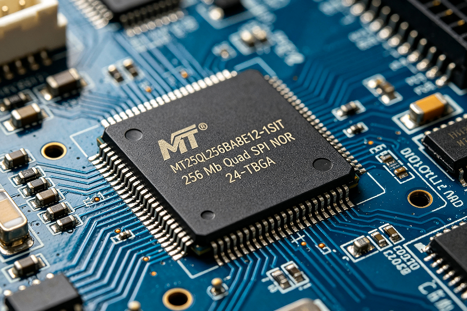
  • MT25QL256ABA8E12 1SIT: 256Mb Four-way SPI Serial NOR Flash Memory for Industrial OEM and EMS Firmware Storage

    MT25QL256ABA8E12‑1SIT: 256Mb quad-channel SPI serial NOR flash memory for industrial OEM and EMS firmware storage Quick Answer ApplicationsMT25QL256ABA8E12‑1SITWhen your bill of materials requires a 256Mb, quad-channel SPI serial NOR flash memory in a compact 24‑TBGA (6 × 8 × 1.2 mm) package, supporting XIP execution in place. This product offers a maximum clock frequency of up to 133 MHz and features industrial-grade performance−40 °C ~ +85 °C operating temperature range; be sure to verify batch status, date code, and lifecycle condition before bulk purchasing. Micron Technology... Introduction MT25QL256ABA8E12‑1SIT is a 256 from Micron... A multi-I/O serial NOR flash memory suitable for storing embedded firmware, boot programs, and configuration parameters. It supports a quad SPI high-speed interface and execute-in-place (XIP) functionality, reducing RAM overhead on microcontroller-based platforms. Mouser Ele.... For electronic component procurement managers and OEM/EMS buyers, its core value lies in combining fast random read performance, industrial-grade environmental robustness, and secure write protection, making it ideal for new product development and ongoing maintenance of frozen BOMs. This product is a surface-mount non-volatile code storage device, not intended for large-scale data file storage. Product Overview and Positioning First, let's present the key conclusion: The MT25QL256ABA8E12‑1SIT is an industrial-grade 256‑bit Mb quad-SPI NOR flash memory, optimized for boot programs and firmware storage, is suitable both for new embedded designs and for maintaining legacy platforms where pin-compatible replacements might pose firmware verification risks. This 24‑TBGA device complies with standard SPI, Dual SPI, and Quad SPI protocols, integrating hardware write protection, an OTP one-time programmable memory area, and CRC data integrity checking. Mouser Ele.... It supports 3-byte and 4-byte address modes to access the full 256 Mb of storage space, and features flexible erase granularity, including 4 KB subsectors, 64 KB sectors, as well as bulk erase operations on the entire chip. The operating supply voltage ranges from 2.7 V to 3.6 V, with a rated industrial temperature range of−40 °C to +85 °C, with a typical data retention period of 20 years at the rated temperature. Although other 256 devices are available on the market... Mb serial NOR devices, but density or the Quad‑SPI interface alone cannot guarantee identical boot timing, write protection behavior, or erase sector characteristics. For any proposed direct replacement solution, engineering validation remains essential. Four Core Advantages of OEM/EMS Embedded Projects Quad‑SPI high-speed interface supporting XIP for immediate execution First, let's state the core conclusion: Up to 133 MHz Quad‑SPI clock enables fast random reads and XIP functionality, reducing the system's RAM requirements for running bootloader and RTOS firmware. The maximum STR clock frequency can reach 133 MHz, while the DTR dual-transfer-rate mode supports 90 MHz, thereby increasing the effective read bandwidth for firmware boot and code execution. XIP allows MCUs or FPGAs to run code directly from flash memory without needing to map the entire image into RAM. Important note: Actual throughput depends on the host controller, PCB signal integrity, and the implementation of the firmware driver; the published clock parameters represent maximum values under laboratory conditions and do not guarantee the system's actual performance. Industrial-grade wide-temperature compact 24‑TBGA package First, let's present the core conclusion: Small size 6 × 8 × 1.2 The 24‑TBGA package size is suitable for space-constrained embedded PCBs and features full industrial-grade specifications−40 °C ~ +85 °C temperature tolerance Micron Technology.... The compact TBGA package is ideally suited for high-density industrial control, IoT, and networking devices. When selecting or replacing components, it is essential to review the package's solder ball array, mechanical height, and reflow soldering process. Its full industrial-grade temperature range supports deployment in factory equipment, outdoor field nodes, and uncontrolled-environment enclosures; however, without official supporting documentation, it does not meet automotive-grade certification requirements. Multi-layered hardware and software security with write protection First, let's present the core conclusion: A rich set of locking mechanisms, including one-time programmable memory, sector-level write protection, and CRC verification, effectively enhances the firmware tamper resistance and data integrity of OEM end products. Mouser Electronics.... This component includes a dedicated 64-byte user-lockable OTP area, used for motherboard serialization, unique ID, or calibration constants. Volatile and non-volatile sector-level locking, a hardware write-protection pin, and a program-erase inhibit feature on power-up effectively prevent accidental or malicious firmware overwrites. The built-in CRC check function helps the host system verify the integrity of the firmware image during startup, thereby reducing field failures caused by bit flips. Flexible erase granularity and long-term data retention First, let's present the core conclusion: Hybrid 4 KB / 64 KB erase granularity optimizes update efficiency; a typical 20-year data retention period ensures long-term storage of configuration and boot code. 4 The KB sub-sector erase function allows partial updates of small-sized configurations without erasing adjacent large sectors, thereby shortening firmware update times for IoT and industrial devices. A typical data retention period of 20 years reduces the risk of configuration loss during the device's service life. When defining the on-site update frequency for end products, it is essential to strictly adhere to programming/erasure endurance and data retention specifications. Technical Parameters and Procurement Interpretation Table Parameter Published Value Procurement Meaning Manufacturer Micron Technology Please verify the complete device suffix, wafer marking, and traceability documents; do not rely solely on the market title "Micron Technology"... Storage Density 256 Mb (32 MB) Confirm the available storage mapping; full-density access requires a 4-byte address mode Interface SPI / Dual SPI / Quad SPI (STR / DTR) The host controller must support Quad SPI to achieve maximum throughput; please verify driver compatibility Maximum Clock Speed 133 MHz (STR), 90 MHz (DTR) Maximum value from laboratory calibration; actual speed depends on PCB layout and host timing margin. Package 24‑TBGA (T‑PBGA) Before evaluating alternative devices, please verify the ball grid array diagram, package outline, and reflow soldering profile. Dimensions 6.0 × 8.0 × 1.2 Millimeter maximum Verify the mechanical height limit of the target enclosure design Operating temperature −40 °C ~ +85 °C Industrial-grade temperature rating; does not meet AEC‑Q100 automotive-grade standards without formal certification Supply voltage 2.7 V ~ 3.6 V Must comply with the design specifications of the circuit board's power rails Erase granularity 4 KB sub-sector, 64 KB sector, bulk erase Firmware partition layout must align with sector boundaries to enable efficient field upgrades Data retention 20 Years (at rated temperature) Plan for the expected end-of-life of deployed devices Note: This table is used for bill of materials screening and quotation preparation. The final engineering release must refer to Micron's official MT25QL256ABA8E12‑1SIT datasheet. Applicable Application Scenarios Industrial Controllers and Human-Machine Interface Devices Industrial human-machine interfaces, PLC auxiliary modules, and embedded controllers all use this NOR flash memory to store boot programs, RTOS firmware, and factory-calibrated parameters. Before mass production, it is necessary to verify the erase-update workload, thermal operating range, power-off recovery process, and write protection configuration. Network Gateways and FPGA-Based Embedded Hardware IoT edge gateways, remote field terminals, and FPGA systems are used to store bitstream configuration images, boot code, and network setting parameters. XIP functionality helps reduce external RAM material costs. For unattended remote hardware, CRC integrity checks should be implemented, and the sampling scope for incoming inspection should be clearly defined. Secure Smart Instruments and Test Equipment Dedicated test and measurement instruments and smart industrial sensors utilize OTP serialization and multi-level write protection mechanisms to ensure the security of firmware images and unit-specific calibration data. Do not select devices solely based on density; be sure to confirm that erase granularity, locking characteristics, and temperature ratings meet the product's safety and reliability requirements. Buyer Pain Points and Practical Countermeasures Pain Points Practical Solutions for OEM/EMS Procurement Suppliers offer "pin-equivalent" alternatives to 256 Mb NOR flash memory as a direct replacement product Compare ball grid array layout, package size, erase sector structure, boot timing, and write protection features; conduct comprehensive firmware verification before modifying the bill of materials The lifecycle and obsolescence risk of MT25QL256ABA8E12‑1SIT remain unclear Require manufacturers to provide channel-level lifecycle declarations and dated quotations; third-party component databases are not authoritative sources for obsolescence notices Existing inventory may include components with earlier production dates and unclear storage histories Review the batch number, MSL status of dry-packaged components, baking records, and solderability risks; establish risk-based incoming inspection sampling plans. The marketing materials state that the maximum frequency is 133. The MHz clock is specified as the guaranteed actual operating frequency. 133 MHz is regarded as the highest specification in the laboratory; communicate reasonable timing margin expectations to the hardware and firmware engineering teams. Brokerage channel inventory lacks complete component traceability. Conduct supplier qualification audits for industrial-grade orders, maintain photo documentation and batch traceability records, and implement a risk-adjusted incoming material inspection process. Lifecycle and Incoming Material Quality Control Guide First, let's clarify the core conclusion.: Before placing a mass-production order for the MT25QL256ABA8E12‑1SIT, please confirm its official lifecycle status. Public third-party component databases may display conflicting supply statuses. Procurement teams must obtain supporting documentation from authorized supplier channels and should not rely solely on aggregated data scraped from the web as official Micron notifications. The actual incoming material control process for MT25QL256ABA8E12‑1SIT includes the following steps: Thorough verification of MPN, suffix, batch number, and date code labels against documentation Visual inspection of packaging and markings Risk-weighted X-ray sampling of older batches to verify ball grid array solder joint conditions Inspection of moisture-sensitive devices using desiccant bags and humidity indicators Planning of reflow/baking processes for inventory with outdated date codes Sampling and validation of electrical, read/write, and startup functions specific to particular applications The level of inspection is adjusted based on supplier risk rating, batch age, total order quantity, and the criticality of the end equipment. Frequently Asked Questions (FAQ) Q1: What is the storage density provided by MT25QL256ABA8E12‑1SIT?A1: It is 256 Mb (32 4‑wire serial NOR flash memory (MB). Full storage capacity requires enabling 4‑byte address mode on the host controller; available capacity depends on the firmware partition layout. Q2: What interface standards does the MT25QL256ABA8E12‑1SIT support?A2: It supports standard SPI, dual SPI, and quad SPI interfaces, as well as single‑data‑rate (STR) and double‑data‑rate (DTR) modes, up to a maximum of 133 MHz STR clock frequency. Q3: Is 133 MHz guaranteed to be the actual operating clock frequency?A3: 133 MHz is the maximum STR clock frequency published by the manufacturer under laboratory conditions. The actual stable operating frequency depends on the host controller's performance, PCB signal integrity, and firmware timing configuration, and must be verified at the system level. Q4: Can any other 256 Mb quad‑channel SPI NOR flash memory directly replace it?A4: No. Differences in pin layout, erase sector size, write protection registers, and start-up timing may cause validated embedded firmware to fail to operate properly. Before approving the use of alternative devices, complete hardware and firmware certification must be performed. Q5: Is it−40 °C ~ +85 Does an operating temperature rating of °C mean that the device has passed automotive-grade AEC‑Q100 certification?A5: An industrial-grade temperature range alone does not equate to automotive-grade certification. If you plan to use this component in automotive systems, be sure to request official certification documents. Q6: What information should be included in the RFQ for MT25QL256ABA8E12‑1SIT?A6: Please submit the complete and accurate MPN number (including the suffix), target quantity, requested delivery date, shipping destination, acceptable date code range, packaging requirements (tray/reel), expectations for traceability documents, inspection standards, and clearly indicate whether alternative component proposals are permitted. Q7: What are the main application areas of MT25QL256ABA8E12‑1SIT?A7: Industrial controllers, human-machine interfaces (HMI), network gateways, FPGA configuration storage, and firmware storage for smart test instruments—suitable for both new industrial designs and continued use on existing qualified platforms. Request a project-specific quotation MT25QL256ABA8E12‑1SIT is best suited for projects requiring 256-bit storage capacity. An industrial-grade, four-channel SPI serial NOR flash memory in a compact 24‑TBGA package, suitable for storing boot programs, firmware, and security configurations. It can be used both for new product development and for the ongoing maintenance of frozen BOMs. Please send your target quantity, required lead time, end-application details, acceptable date-code constraints, and incoming inspection requirements to our sales team. Before placing a purchase order, please confirm the specific device's availability, batch traceability, packaging condition, and formal delivery terms. Technical Documentation Sources Official datasheet for Micron's MT25QL256ABA series. View Micron's hardware integration application notes for serial NOR flash memory. View source